| CPC H01L 23/50 (2013.01) [H01L 25/072 (2013.01)] | 6 Claims |
|
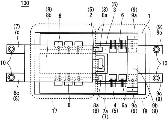
1. A semiconductor device, comprising:
an insulating substrate;
a circuit pattern including a circuit pattern on a low potential side provided on the insulating substrate and a circuit pattern on a high potential side provided in a region adjacent to the circuit pattern on the low potential side on the insulating substrate;
a plurality of semiconductor chips mounted on the circuit pattern;
a low potential terminal having one end portion connected to the circuit pattern on the low potential side; and
a high potential terminal having one end portion connected to the circuit pattern on the high potential side, wherein
the insulating substrate is a single insulating substrate, and
the high potential terminal and the low potential terminal include a midway portion constituting parallel flat plates vertical disposed in parallel to each other and extending on a side of the circuit pattern on the low potential side and another end portion protruding from the insulating substrate.
|