| CPC H01L 23/49838 (2013.01) [H01L 21/481 (2013.01); H01L 21/486 (2013.01); H01L 22/14 (2013.01); H01L 23/49827 (2013.01); H01L 23/5384 (2013.01); H01L 23/5386 (2013.01); H01L 23/4985 (2013.01); H01L 23/5387 (2013.01); H01L 25/18 (2013.01)] | 20 Claims |
|
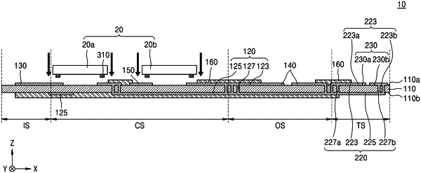
1. A package substrate film, comprising:
a film substrate including an upper surface and a lower surface;
a chip bonding pad on a chip section of the film substrate; and
a test pattern on a test section of the film substrate such that the entire test pattern is between the chip bonding pad and one outer edge of the film substrate, the test pattern including:
an upper test line pattern extending on the upper surface of the film substrate;
a lower test line pattern extending on the lower surface of the film substrate;
a first test via pattern penetrating the film substrate and connecting the upper test line pattern to the lower test line pattern;
a second test via pattern penetrating the film substrate at an outer side of the first test via pattern such that the first test via pattern is between the chip bonding pad and the second test via pattern, the second test via pattern connecting the upper test line pattern to the lower test line pattern; and
a test pad between the first test via pattern and the second test via pattern, the test pad including at least one first test pad at an outer side of the first test via pattern; and at least one second test pad at an inner side of the second test via pattern and facing the at least one first test pad.
|