| CPC H01L 23/49555 (2013.01) [H01L 21/561 (2013.01); H01L 23/3107 (2013.01); H01L 23/3114 (2013.01); H01L 23/4012 (2013.01); H01L 23/42 (2013.01); H01L 23/49503 (2013.01); H01L 23/49562 (2013.01); H01L 24/24 (2013.01); H01L 24/25 (2013.01); H01L 24/73 (2013.01); H01L 24/82 (2013.01); H01L 25/16 (2013.01); H01L 2924/181 (2013.01)] | 17 Claims |
|
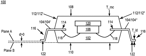
1. A molded semiconductor package, comprising:
a mold compound;
a plurality of leads, each lead of the plurality of leads having a first end embedded in the mold compound and a second end protruding from a side face of the mold compound; and
a semiconductor die embedded in the mold compound and electrically connected, within the mold compound, to the plurality of leads,
wherein the second end of each lead of the plurality of leads has a bottom surface facing in a same direction as a bottom main surface of the mold compound,
wherein each lead of the plurality of leads has a negative standoff relative to the bottom main surface of the mold compound, and
wherein the mold compound has a height tolerance of 100 μm or less.
|