| CPC H01L 23/481 (2013.01) [H01L 21/308 (2013.01); H01L 21/76804 (2013.01); H01L 21/76831 (2013.01); H01L 21/76898 (2013.01); H01L 23/5226 (2013.01)] | 20 Claims |
|
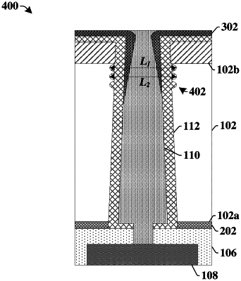
1. An integrated chip, comprising:
a semiconductor device arranged along a first side of a semiconductor substrate, wherein the semiconductor substrate comprises one or more sidewalls extending from the first side of the semiconductor substrate to an opposing second side of the semiconductor substrate;
a dielectric liner lining the one or more sidewalls of the semiconductor substrate;
a through-substrate-via (TSV) arranged between the one or more sidewalls and separated from the semiconductor substrate by the dielectric liner; and
wherein the dielectric liner has sidewalls that slope inward towards one another from an upper surface of the dielectric liner arranged directly below the TSV to a topmost surface of the dielectric liner over the one or more sidewalls of the semiconductor substrate, so that the dielectric liner overhangs the TSV in a cross-sectional view.
|