| CPC H01L 21/76885 (2013.01) [C23C 18/1605 (2013.01); C23C 18/1651 (2013.01); C25D 5/022 (2013.01); C25D 5/10 (2013.01); C25D 7/123 (2013.01); H01L 21/0331 (2013.01); H01L 21/2885 (2013.01); H01L 21/76846 (2013.01); H01L 21/76852 (2013.01); H01L 21/76873 (2013.01); H01L 23/5226 (2013.01); H01L 23/53238 (2013.01); H01L 28/10 (2013.01); H05K 3/184 (2013.01); H05K 3/244 (2013.01); H05K 3/422 (2013.01); H05K 1/0265 (2013.01); H05K 3/188 (2013.01); H05K 3/424 (2013.01); H05K 2201/0367 (2013.01); H05K 2201/0391 (2013.01); H05K 2201/096 (2013.01); H05K 2201/09563 (2013.01); H05K 2201/09845 (2013.01); H05K 2203/0716 (2013.01); H05K 2203/1407 (2013.01); H05K 2203/1423 (2013.01); H05K 2203/1476 (2013.01)] | 19 Claims |
|
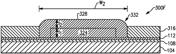
1. A method of metallizing an integrated circuit device, comprising:
plating a first metal on a substrate in a first opening formed through a first masking layer, the first opening defining a first region of the substrate;
removing the first masking layer from the substrate;
after removing the first masking layer from the substrate, forming a second masking layer on the substrate; and
plating a second metal on the substrate in a second opening formed through the second masking layer, the second opening defining a second region of the substrate, wherein the second opening is wider than the first opening and the second region encompasses the first region of the substrate, and wherein plating the first metal forms a first metal feature and plating the second metal encapsulates the first metal feature to form a metallization structure that has a thickness greater than each of a thickness of the first masking layer and a thickness of the second masking layer; and
after plating the second metal on the substrate, removing the second masking layer.
|