| CPC H01L 21/76877 (2013.01) [G11C 11/221 (2013.01); H01L 21/76802 (2013.01); H01L 23/5384 (2013.01); H10B 53/20 (2023.02)] | 20 Claims |
|
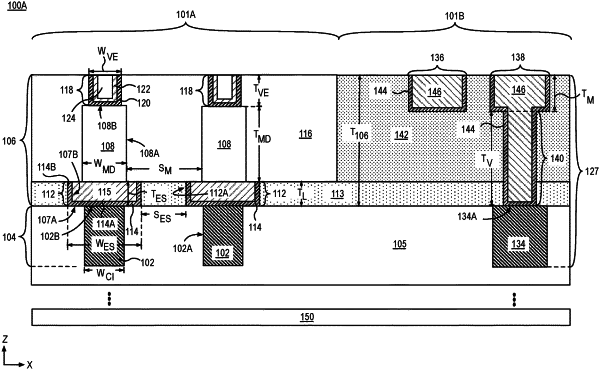
1. A device comprising:
a first region comprising:
a first conductive interconnect within a first dielectric in a first level;
a second level above the first level, the second level comprising:
a first electrode structure on at least a portion of the first conductive interconnect, the first electrode structure comprising:
a first conductive hydrogen barrier layer; and
a first conductive fill material adjacent to the first conductive hydrogen barrier layer;
an insulator layer laterally surrounding the first electrode structure; and
a memory device on least a portion of the first electrode structure, the memory device comprising a ferroelectric material or a paraelectric material;
a second dielectric spanning the first region and on the insulator layer, the second dielectric comprising an amorphous, greater than 90% film density hydrogen barrier material, wherein the memory device is directly adjacent to and embedded within the second dielectric;
a third dielectric comprising a less than 90% film density material on the second dielectric, the third dielectric within a third level above the second level;
a second electrode structure coupled with the memory device, the second electrode structure comprising:
a via electrode on at least a portion of the memory device and adjacent to the second dielectric;
a trench electrode on the via electrode, the trench electrode adjacent to the third dielectric;
a second conductive hydrogen barrier layer comprising:
a lateral portion on the memory device;
first substantially vertical portions directly adjacent to the second dielectric; and
second substantially vertical portions directly adjacent to the third dielectric; and
a second conductive fill material that extends continuously from the lateral portion to a first uppermost surface of the third dielectric; and
a second region adjacent to the first region, the second region comprising:
a fourth dielectric comprising dielectric comprising a first less than 90% film density material directly adjacent to the second dielectric and below the third dielectric;
a second conductive interconnect within the first level;
a third conductive interconnect within the third level, wherein the third dielectric extends over the fourth dielectric and wherein the third dielectric laterally surrounds the third conductive interconnect; and
a via structure coupled between the second conductive interconnect and the third conductive interconnect, wherein at least a first portion of the via structure is adjacent to the insulator layer.
|