| CPC H01L 21/7682 (2013.01) [H01L 21/76831 (2013.01); H01L 21/76834 (2013.01); H01L 21/76877 (2013.01); H01L 23/5226 (2013.01); H01L 23/5329 (2013.01); H01L 21/76895 (2013.01); H01L 23/28 (2013.01); H01L 23/48 (2013.01); H10B 12/482 (2023.02)] | 20 Claims |
|
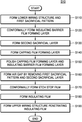
1. A method of manufacturing an integrated circuit device, the method comprising:
forming a lower wiring structure and a first sacrificial pattern on the lower wiring structure;
conformally forming an insulating barrier layer on the lower wiring structure and the first sacrificial pattern;
forming a second sacrificial pattern to fill a portion of an opening defined by the insulating barrier layer;
forming a capping layer on the second sacrificial pattern and the insulating barrier layer;
polishing the capping layer and the insulating barrier layer until an upper surface of the first sacrificial pattern is exposed;
removing the first sacrificial pattern;
forming an air gap by removing the second sacrificial pattern;
conformally forming an etch stop layer on the lower wiring structure, the insulating barrier layer, and the capping layer;
forming an insulating layer on the etch stop layer; and
forming an upper wiring structure penetrating the insulating layer.
|