| CPC H01L 21/76297 (2013.01) [H01L 21/02595 (2013.01)] | 20 Claims |
|
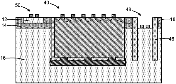
1. A structure comprising:
a semiconductor substrate including a device layer, a buried insulator layer, a handle substrate separated from the device layer by the buried insulator layer, and a first trench that penetrates through the device layer and the buried insulator layer into the handle substrate;
a trench isolation region positioned in the first trench, the trench isolation region comprising a dielectric material, the trench isolation region including a second trench surrounded by the dielectric material, and the trench isolation region including a plurality of openings that penetrate through the dielectric material to the handle substrate; and
a semiconductor layer positioned in the second trench of the trench isolation region, the semiconductor layer comprising a single-crystal semiconductor material.
|