| CPC H01L 21/67282 (2013.01) [H01L 21/0275 (2013.01); H01L 23/528 (2013.01); H01L 23/544 (2013.01); H01L 2223/5444 (2013.01)] | 20 Claims |

|
1. A device with authentication, the device comprising:
a die formed of a semiconductor substrate and containing an integrated circuit, the die having a plurality of field-effect transistors and multiple wiring levels, the multiple wiring levels having been patterned using a mask-based photolithography system; and
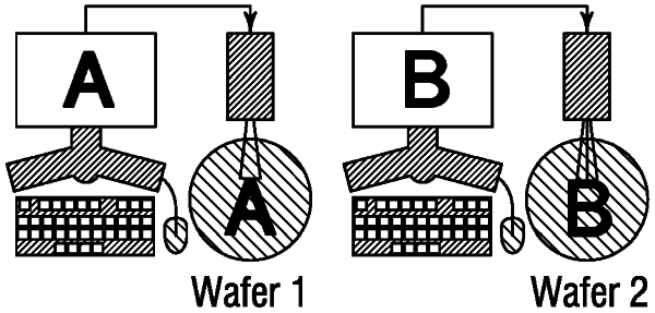
a unique wiring structure formed on a predetermined region of the die, the unique wiring structure having been patterned using a direct-write projection system, the unique wiring structure having a unique electrical signature that identifies the die relative to other dies,
wherein the unique wiring structure is positioned on the predetermined region which is separated from die circuitry.
|