US 11,862,492 B2
Apparatus, system, and method of providing a ramped interconnect for semiconductor fabrication
Lim Lai Ming, Penang (MY); and Zambri Bin Samsudin, Penang (MY)
Assigned to JABIL INC., St. Petersburg, FL (US)
Filed by JABIL INC., St. Petersburg, FL (US)
Filed on Aug. 2, 2021, as Appl. No. 17/391,120.
Application 17/391,120 is a continuation of application No. 17/003,595, filed on Aug. 26, 2020, granted, now 11,081,375.
Application 17/003,595 is a continuation of application No. 16/104,716, filed on Aug. 17, 2018, granted, now 10,790,172, issued on Sep. 29, 2020.
Prior Publication US 2022/0093424 A1, Mar. 24, 2022
This patent is subject to a terminal disclaimer.
Int. Cl. H01L 21/67 (2006.01); C23C 18/08 (2006.01); H01L 21/48 (2006.01)
CPC H01L 21/67138 (2013.01) [C23C 18/08 (2013.01); H01L 21/485 (2013.01)] 16 Claims
OG exemplary drawing
 
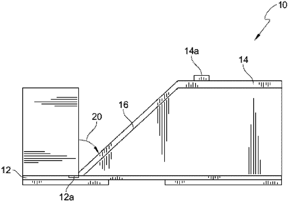
1. An electrical interconnection system, comprising:
a first semiconductor substrate having thereon a first electrical circuit comprising first electrical components; a second semiconductor substrate at least partially covering the first electrical circuit, and having thereon a second electrical circuit comprising second electrical components;
a machined ramp passing through the second semiconductor substrate between one of the first electrical components and one of the second electrical components; and a 3D printed conductive trace formed on the machined ramp to electrically connect the one first electrical component and the one second electrical component.