| CPC H01L 21/4814 (2013.01) [H01L 21/6835 (2013.01); H01L 23/3121 (2013.01); H01L 23/49822 (2013.01); H01L 23/49838 (2013.01); H01L 23/544 (2013.01); H01L 23/552 (2013.01); H01L 2221/6835 (2013.01); H01L 2221/68322 (2013.01); H01L 2223/54413 (2013.01)] | 25 Claims |
|
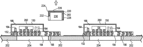
1. A semiconductor device, comprising:
a semiconductor package including,
a substrate comprising a land grid array,
a component disposed over the substrate, and
an encapsulant deposited over the component, wherein the land grid array remains outside the encapsulant;
a carrier, wherein the semiconductor package is disposed on the carrier;
a metal mask including a fiducial marker disposed on the carrier and extending over the land grid array; and
a shielding layer formed over the semiconductor package and metal mask.
|