| CPC H01L 21/34 (2013.01) [H01L 21/02 (2013.01); H01L 21/28 (2013.01); H10B 12/053 (2023.02); H10B 12/31 (2023.02); H10B 12/482 (2023.02)] | 16 Claims |
|
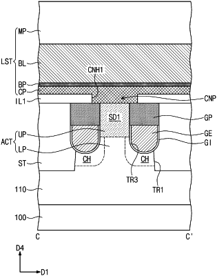
1. A method of forming a semiconductor device comprising:
forming a lower oxide semiconductor layer having a first atomic concentration of oxygen on a semiconductor substrate by sputtering a target including an amorphous oxide semiconductor in a chamber at a first partial pressure of oxygen;
forming an upper oxide semiconductor layer having a second atomic concentration of oxygen that is greater than the first atomic concentration of oxygen, on the lower oxide semiconductor layer by sputtering the target in the chamber at a second partial pressure of oxygen that is greater than the first partial pressure of oxygen, and
forming active patterns in the lower oxide semiconductor layer and the upper oxide semiconductor layer by patterning the upper oxide semiconductor layer and the lower oxide semiconductor layer such that each active pattern comprises:
a lower portion having the first atomic concentration of oxygen, and
an upper portion having the second atomic concentration of oxygen that is greater than the first atomic concentration of oxygen,
wherein the lower portion forms a channel region and the upper portion forms a source/drain region.
|