| CPC H01L 21/02378 (2013.01) [C30B 25/04 (2013.01); C30B 25/183 (2013.01); H01L 21/0242 (2013.01); H01L 21/0254 (2013.01); H01L 21/0262 (2013.01); H01L 21/0265 (2013.01); H01L 21/02381 (2013.01); H01L 21/02458 (2013.01); H01L 21/02502 (2013.01); H01L 21/02603 (2013.01); H01L 21/02647 (2013.01); H01L 33/007 (2013.01); H01L 33/12 (2013.01); H01L 33/16 (2013.01)] | 4 Claims |
|
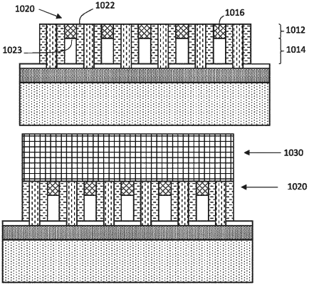
1. A method of fabricating a semiconductor device having a planar III-N semiconductor layer, comprising:
providing a substrate comprising a wafer, a buffer layer of a different material than the wafer, having a growth surface with a first lattice constant at the growth surface, and a mask layer on the growth surface, having an array of nanosized apertures;
epitaxially growing III-N material in the nanosized apertures to form nanostructures, the nanostructures comprising at least one III-N layer with a second lattice constant,
coalescing the nanostructures at an elevated temperature (T) to form a continuous layer, wherein the step of coalescing includes:
releasing column III material from upper ends of the nanostructures; and
filling out a spacing between the nanostructures by forming semiconductor material from the released column III material; and
epitaxially growing a III-N growth layer on said continuous layer;
wherein the III-N growth layer is configured such that thermal expansion between room temperature (RT) and T of the growth layer is different from the wafer; and
wherein a number of lattice cells spanning a distance between adjacent apertures is different at the growth surface of the buffer layer and at the continuous layer.
|