| CPC H01L 21/02057 (2013.01) [B08B 3/08 (2013.01); H01L 21/428 (2013.01); H01L 21/68764 (2013.01)] | 15 Claims |
|
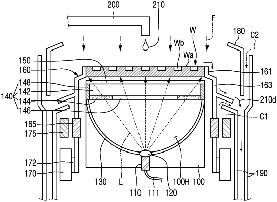
1. A method of fabricating a semiconductor device, the method comprising:
disposing a wafer on a rotatable chuck;
irradiating a lower surface of the wafer with a laser to heat the wafer; and
supplying a chemical to an upper surface of the wafer to clean the wafer,
wherein the laser penetrates an optical system including an aspheric lens array,
wherein the laser penetrates a calibration window, which includes a first window structure including a first light projection window including first and second regions different from each other, a first coating layer covering the first region of the first light projection window, and a second coating layer covering the second region of the first light projection window,
wherein the first coating layer and the second coating layer have different light transmissivities from each other,
wherein the first coating layer surrounds the second coating layer, and
wherein a first light transmissivity of the first coating layer is smaller than a second light transmissivity of the second coating layer.
|