| CPC H01L 21/02057 (2013.01) [H01L 21/02013 (2013.01)] | 8 Claims |
|
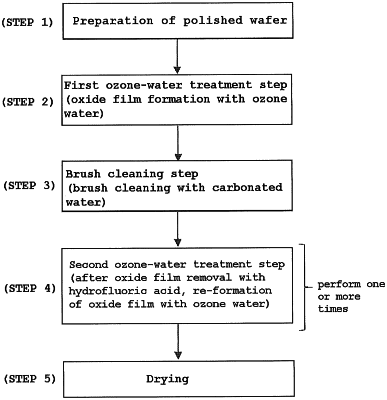
1. A method for cleaning a semiconductor wafer to clean a semiconductor wafer after polishing, the method comprising:
performing a first ozone-water treatment step of cleaning the polished semiconductor wafer with ozone water to form an oxide film;
performing a brush cleaning step of brush-cleaning the semiconductor wafer with carbonated water having a concentration of 100 ppm or more and 1000 ppm or less after the first ozone-water treatment step; and
then performing a second ozone-water treatment step including cleaning the semiconductor wafer with hydrofluoric acid to remove the oxide film, followed by cleaning with ozone water to form an oxide film again, wherein the second ozone-water treatment step is performed one or more times.
|