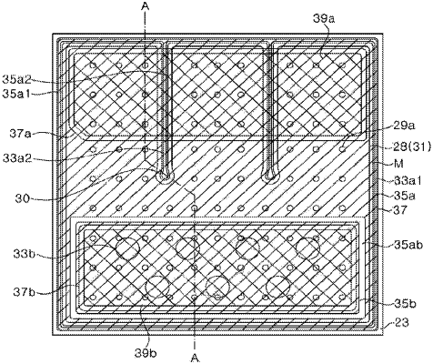
| CPC H01L 33/382 (2013.01) [H01L 33/20 (2013.01); H01L 33/405 (2013.01); H01L 33/44 (2013.01); H01L 33/32 (2013.01)] | 20 Claims |

|
1. A light emitting device, comprising:
a first conductivity type semiconductor layer;
a mesa disposed on the first conductivity type semiconductor layer, and including an active layer and a second conductivity type semiconductor layer;
an ohmic layer disposed on the mesa and electrically connected to the second conductivity type semiconductor layer;
a metal reflection layer disposed to be in contact with the ohmic layer;
a lower insulation layer covering the mesa and the metal reflection layer, and including a first opening exposing the first conductivity type semiconductor layer and a second opening exposing the metal reflection layer;
a first pad metal layer disposed on the lower insulation layer, and electrically connected to the first conductivity type semiconductor layer through the first opening;
a second pad metal layer disposed on the lower insulation layer, and electrically connected to the metal reflection layer through the second opening; and
an upper insulation layer covering the first pad metal layer and the second pad metal layer, and including a third opening exposing the first pad metal layer and a fourth opening exposing the second pad metal layer,
wherein the second pad metal layer is surrounded by the first pad metal layer and a boundary region in which at least a part of the lower insulation layer is exposed is disposed between the first pad metal layer and the second pad metal layer, and
wherein the boundary region is covered by the upper insulation layer.
|