| CPC H01L 29/7869 (2013.01) [H01L 21/0234 (2013.01); H01L 21/0262 (2013.01); H01L 21/02323 (2013.01); H01L 21/02337 (2013.01); H01L 21/02554 (2013.01); H01L 21/02565 (2013.01); H01L 21/02631 (2013.01); H01L 21/425 (2013.01); H01L 27/1225 (2013.01); H01L 29/41733 (2013.01); H01L 29/42384 (2013.01); H01L 29/4908 (2013.01); H01L 29/66742 (2013.01); H01L 29/66969 (2013.01); H01L 29/78696 (2013.01); H01L 21/473 (2013.01); H01L 21/76826 (2013.01); H01L 21/76832 (2013.01)] | 14 Claims |
|
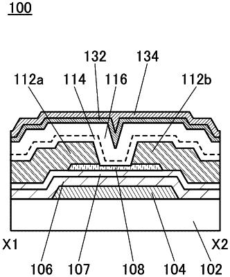
1. A semiconductor device comprising:
an oxide semiconductor film;
a source electrode electrically connected to the oxide semiconductor film;
a drain electrode electrically connected to the oxide semiconductor film;
an insulating film over the oxide semiconductor film, the source electrode, and the drain electrode;
a first metal oxide film over the insulating film; and
a second metal oxide film over the first metal oxide film,
wherein the first metal oxide film comprises at least one metal element included in the oxide semiconductor film,
wherein a mixed region exists between the first metal oxide film and the second metal oxide film,
wherein the mixed region comprises an element included in the first metal oxide film and an element included in the second metal oxide film,
wherein the first metal oxide film comprises In, and
wherein the second metal oxide film comprises Al.
|