| CPC H01J 37/32715 (2013.01) [H01J 37/32541 (2013.01); H01J 37/32568 (2013.01); H01L 21/6833 (2013.01); H01J 37/32697 (2013.01)] | 18 Claims |
|
1. Semiconductor processing equipment comprising:
an upper electrode;
a gas supplier connected to the upper electrode; and
a substrate supporting structure spaced apart from the upper electrode, to define a processing volume, the substrate supporting structure supporting a substrate, wherein:
the substrate supporting structure includes:
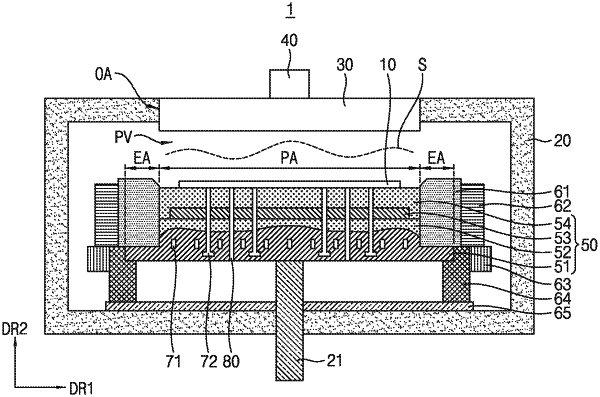
a lower electrode comprising a side area disposed outside a step formed at an outer perimeter portion of the lower electrode and a processing area disposed inside the step;
a first plate disposed on the lower electrode;
an attraction electrode disposed on the first plate; and
a second plate disposed on the attraction electrode, the second plate supporting the substrate in a state in which the substrate is laid on an upper surface of the second plate,
each of the first plate and the second plate comprises ceramic,
an upper surface of the lower electrode is non-planar and has a maximum height aligned with a central portion of the processing area, and
the upper surface of the lower electrode comprises a first peak disposed at the central portion of the processing area, a second peak disposed outside the first peak, and a valley disposed between the first peak and the second peak, when viewed in cross-section.
|