| CPC H01J 37/32495 (2013.01) [C23C 16/45565 (2013.01); H01J 37/3244 (2013.01); H01J 37/32623 (2013.01); H01J 37/3255 (2013.01); H01J 37/32091 (2013.01)] | 12 Claims |
|
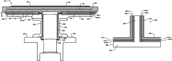
1. A method for creating a high impedance path for reducing parasitic plasma in a process chamber including an electrode and a conducting structure, the method comprising:
selecting a number of a plurality of dielectric layers to arrange between the electrode and a first surface of the conducting structure;
selecting respective sizes of (i) a first gap between the electrode and a first one of the plurality of dielectric layers, (ii) a second gap between adjacent ones of the plurality of dielectric layers, and (iii) a third gap between a last one of the plurality of dielectric layers and the first surface,
wherein selecting the number of the plurality of dielectric layers and the respective sizes includes selecting the number of the plurality of dielectric layers and the respective sizes to prevent parasitic plasma between the first surface and the electrode during a semiconductor process performed in the process chamber; and
vertically arranging the selected number of the plurality of dielectric layers in a vertical stack between the electrode and the first surface of the conducting structure in accordance with the selected respective sizes of the first gap, the second gap, and the third gap.
|