| CPC H01J 37/3175 (2013.01) [B29C 33/3842 (2013.01); G03F 7/0002 (2013.01); H01J 2237/31777 (2013.01)] | 20 Claims |

|
1. A pattern formation method, comprising:
placing an imprint resist film on a substrate;
imprinting a pattern in the imprint resist film, the pattern having a first loop section in a first end portion and a second loop section in a second end portion;
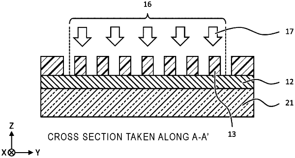
selectively irradiating the patterned imprint resist film between the first loop section and the second loop section; and
etching the imprint resist film under conditions leaving the selectively irradiated portion of the imprint resist film and removing the unirradiated portion of the imprint resist film.
|
|
9. A patterning method, comprising:
obtaining a first imprint template including a line and space pattern formed by a side wall transfer process, the line and space pattern including a first loop end portion at one end and a second loop end portion at another end;
performing an imprint lithography process on a substrate using the first imprint template to transfer the line and space pattern to an imprint resist on the substrate;
after the imprint lithography process, radiation hardening a portion of the imprint resist between the first loop end portion and the second loop end portion;
etching the imprint resist to remove the portions of the imprint resist that were not radiation hardened and leave the portions of the imprint resist that were radiation hardened; and
etching the substrate using the remaining portions of the radiation hardened imprint resist as a mask.
|
|
16. A template manufacturing method, comprising:
forming a hard mask film on a substrate;
forming a resist film on the hard mask film;
patterning the resist film to have a pattern including a first loop section in a first end portion of a line-space pattern and a second loop section in a second end portion of the line-space pattern;
irradiating the resist between the first loop section and the second loop section;
removing the portions of the resist not irradiated; and
etching the mask film and the substrate using the remaining resist film.
|