| CPC H01H 47/32 (2013.01) | 3 Claims |
|
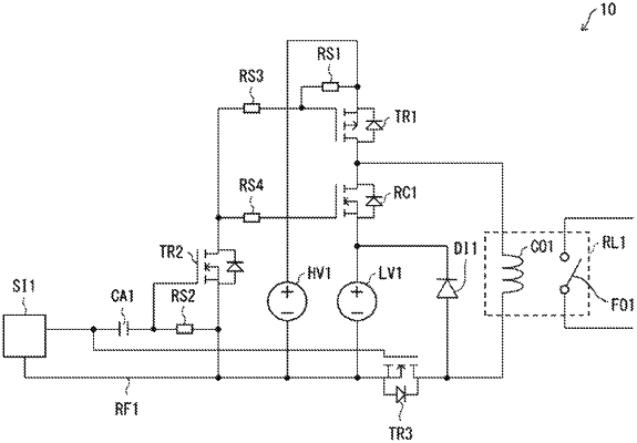
1. A relay control circuit configured to control opening and closing of a contact of a non-latch relay, the non-latch relay including the contact and a coil configured to operate the contact, the relay control circuit comprising:
a low-voltage power supply;
a high-voltage power supply;
a first transistor;
a second transistor;
a rectifying element; and
a reference voltage node,
wherein a high-voltage terminal of the first transistor is connected to a positive electrode of the high-voltage power supply,
a low-voltage terminal of the first transistor is connected to one end of the coil,
an anode of the rectifying element is connected to a positive electrode of the low-voltage power supply,
a cathode of the rectifying element is connected to the one end of the coil,
a negative electrode of the high-voltage power supply, a negative electrode of the low-voltage power supply, and another end of the coil are connected to the reference voltage node,
a low-voltage terminal of the second transistor is connected to the reference voltage node,
a high-voltage terminal of the second transistor is connected to a control terminal of the first transistor,
the control terminal of the first transistor is connected to the positive electrode of the high-voltage power supply via a first resistor,
in a case that the second transistor is turned on, the first transistor is also turned on, and in a case that the second transistor is turned off, the first transistor is also turned off,
the rectifying element is an N-channel metal-oxide semiconductor (NMOS), and
a control terminal of the NMOS is connected to the high-voltage terminal of the second transistor, such that a voltage of the control terminal of the NMOS is lower than a voltage of an anode of the NMOS by an amount of voltage that is equal to a voltage of the low-voltage power supply in a case that the second transistor is turned on.
|