| CPC H01G 4/232 (2013.01) [H01G 2/065 (2013.01); H01G 4/012 (2013.01); H01G 4/1227 (2013.01); H01G 4/224 (2013.01); H01G 4/33 (2013.01); H01G 13/00 (2013.01)] | 18 Claims |
|
1. A multilayer capacitor, comprising:
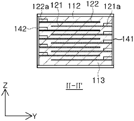
a capacitor body comprising first and second dielectric layers and first and second internal electrodes, and a first surface and a second surface opposing each other, a third surface and a fourth surface connected to the first and second surfaces and opposing each other, and a fifth surface and a sixth surface connected to the first to fourth surfaces and opposing each other, the first internal electrode being exposed through the third surface and the fifth surface and the second internal electrode being exposed through the fourth surface and the sixth surface;
first and second side portions disposed on the fifth and sixth surfaces, respectively, of the capacitor body;
first and second external electrodes respectively disposed on the third and fourth surfaces of the capacitor body and respectively connected to the first and second internal electrodes;
a first protrusion disposed on a first margin portion in a width direction on the second dielectric layer on which the second internal electrode is disposed, the first protrusion being disposed on the first internal electrode; and
a second protrusion disposed on a second margin portion in the width direction on the first dielectric layer on which the first internal electrode is disposed, the second protrusion being disposed on the second internal electrode,
wherein an average thickness of each of the first and second internal electrodes is 0.41 μm or less.
|