| CPC H01G 4/012 (2013.01) [H01G 4/232 (2013.01); H01G 4/30 (2013.01)] | 18 Claims |
|
1. A multilayer ceramic capacitor comprising:
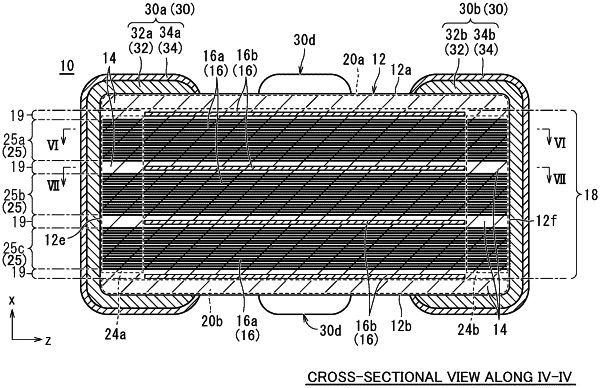
a multilayer body including a plurality of layered dielectric layers, the multilayer body including a first main surface and a second main surface opposed to each other in a height direction, a first end surface and a second end surface opposed to each other in a length direction orthogonal to the height direction, and a first side surface and a second side surface opposed to each other in a width direction orthogonal to the height direction and the length direction;
a plurality of first internal electrode layers on the plurality of dielectric layers and drawn to the first end surface and the second end surface;
a plurality of second internal electrode layers on the plurality of dielectric layers and drawn to the first side surface and the second side surface;
a first external electrode on the first end surface and connected to the first internal electrode layers;
a second external electrode on the second end surface and connected to the first internal electrode layers;
a third external electrode on the first side surface and connected to the second internal electrode layers; and
a fourth external electrode on the second side surface and connected to the second internal electrode layers; wherein
each of the second internal electrode layers includes a central section located in a central portion of the dielectric layer and an extending section that extends from the central section located in the central portion of the dielectric layer to the first side surface and the second side surface;
the first internal electrode layers are larger in number than the second internal electrode layers, at least two of the first internal electrode layers are successively layered, and the extending section is larger in thickness than the central section located in the central portion of the dielectric layer; and
a thickness of the extending section of each of the second internal electrode layers is larger than a thickness of each of the first internal electrode layers.
|