| CPC H01G 4/0085 (2013.01) [H01G 4/30 (2013.01); H01G 4/1227 (2013.01)] | 6 Claims |
|
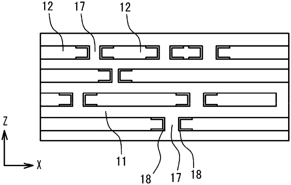
1. A ceramic electronic device comprising:
a multilayer structure in which each of a plurality of dielectric layers including Ba and Ti and each of a plurality of internal electrode layers including Ni and Sn are alternately stacked,
wherein a discontinuity is formed in at least one of the plurality of internal electrode layers, the discontinuity being a break in a cross section including a stacking direction of the multilayer structure, and
wherein an Sn high concentration portion, of which an Sn concentration is higher than an average Sn concentration of the one of the internal electrode layers, is formed on a part of a surface of the at least one of the internal electrode layers, the part of the surface being exposed to the discontinuity.
|