| CPC H01F 27/292 (2013.01) [H01F 27/2804 (2013.01); H01F 27/327 (2013.01); H01F 27/346 (2013.01); H01F 41/041 (2013.01); H01F 2027/2809 (2013.01)] | 13 Claims |
|
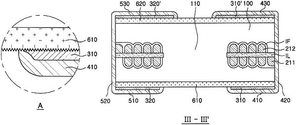
1. A coil component comprising:
a body having a first surface and a second surface opposing each other in a thickness direction of the body and including a core formed in the thickness direction;
a coil part embedded in the body and comprising at least one turn around the core;
a first insulating layer disposed on the first surface of the body;
a first bonded conductive layer disposed on the first insulating layer and having a surface roughness of a first surface which is in contact with the first insulating layer greater than a surface roughness of a second surface opposing the first surface of the first bonded conductive layer;
a second insulating layer disposed on the second surface of the body;
a second bonded conductive layer disposed on the second insulating layer; and
external electrodes connected to the coil part and covering the first bonded conductive layer and the second bonded conductive layer,
wherein the body further has end surfaces opposing each other while connecting the first surface and the second surface of the body to each other, and
the end surfaces of the body are free of each of the first insulating layer, the first bonded conductive layer, the second insulating layer, and the second bonded conductive layer.
|