| CPC H01F 27/29 (2013.01) [H01F 27/06 (2013.01); H01F 27/2804 (2013.01); H01R 12/57 (2013.01); H03H 1/0007 (2013.01); H05K 1/181 (2013.01); H01F 2027/065 (2013.01); H01F 2027/2814 (2013.01); H01R 24/64 (2013.01); H03H 2001/0092 (2013.01); H05K 2201/1006 (2013.01); H05K 2201/10522 (2013.01)] | 20 Claims |
|
1. An electromagnetic device, comprising:
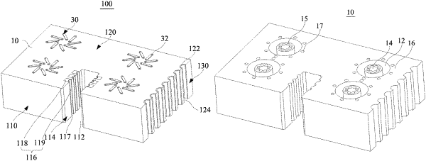
a substrate defining a plurality of annular receiving grooves, wherein each annular receiving groove divides the substrate into a central portion surrounded by the annular receiving groove and a peripheral portion surrounding the annular receiving groove, each central portion defines a plurality of inner via holes running through the substrate, and each peripheral portion defines a plurality of outer via holes running through the substrate;
a plurality of magnetic cores each received in the plurality of annular receiving grooves;
at least two transmission line layers, wherein each of two opposite sides of the substrate is provided with one of the transmission line layers, each transmission line layer comprises a plurality of wire patterns arranged spacedly, and each wire pattern is bridged between one of the inner via holes and one of the outer via holes corresponding to each other; and
a plurality of conductive members, which are respectively disposed in each of the inner via holes and each of the outer via holes, and are configured to sequentially connect the wire patterns on the two transmission line layers so as to form a coil circuit capable of surrounding the magnet cores;
wherein, the plurality of central portions on the substrate, the peripheral portions corresponding thereto, the plurality of magnet cores, the plurality of conductive members, and the transmission line layers located at the two opposite sides of the substrate form a plurality of transformers and/or a plurality of filters;
wherein, the electromagnetic device further comprises a first side surface being perpendicular to the transmission line layers, the first side surface is provided with an insertion slot, the insertion slot runs through the electromagnetic device along an axial direction of one of the inner via holes, and the insertion slot is configured to fix and connect a first adapter plate.
|