US 11,862,373 B2
MRAM stacks and memory devices
Shy-Jay Lin, Hsinchu County (TW); Wilman Tsai, Saratoga, CA (US); and Ming-Yuan Song, Hsinchu (TW)
Assigned to Taiwan Semiconductor Manufacturing Company, Ltd., Hsinchu (TW)
Filed by Taiwan Semiconductor Manufacturing Company, Ltd., Hsinchu (TW)
Filed on Jul. 29, 2022, as Appl. No. 17/876,587.
Application 17/876,587 is a continuation of application No. 16/805,863, filed on Mar. 2, 2020, granted, now 11,456,100.
Claims priority of provisional application 62/849,163, filed on May 17, 2019.
Prior Publication US 2022/0367098 A1, Nov. 17, 2022
Int. Cl. H01F 10/32 (2006.01); G11C 11/16 (2006.01); H01F 41/32 (2006.01); H10B 61/00 (2023.01); H10N 50/01 (2023.01); H10N 50/80 (2023.01); H10N 50/85 (2023.01)
CPC H01F 10/329 (2013.01) [G11C 11/161 (2013.01); H01F 10/3259 (2013.01); H01F 10/3286 (2013.01); H01F 41/32 (2013.01); H10B 61/22 (2023.02); H10N 50/01 (2023.02); H10N 50/80 (2023.02); H10N 50/85 (2023.02)] 19 Claims
OG exemplary drawing
 
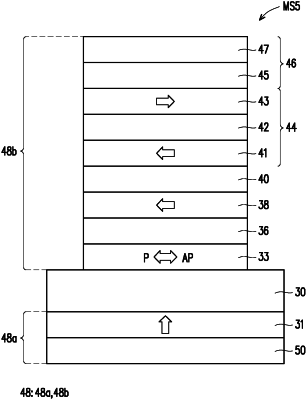
1. A memory stack, comprising:
a spin-orbit torque layer;
a magnetic bias layer disposed below the spin-orbit torque layer and having a first magnetic anisotropy; and
a free layer disposed above the spin-orbit torque layer and having a second magnetic anisotropy perpendicular to the first magnetic anisotropy,
wherein a width of the magnetic bias layer is different from a width of the free layer.