| CPC G11C 7/08 (2013.01) [G11C 7/12 (2013.01)] | 17 Claims |
|
1. A sense amplifier, comprising:
a first positive channel metal oxide semiconductor (PMOS) transistor, a gate of the first PMOS transistor being connected to a first bit line;
a second PMOS transistor, a gate of the second PMOS transistor being connected to a second bit line, and a source of the second PMOS transistor being connected to a source of the first PMOS transistor, wherein the second bit line is an inverse bit line corresponding to the first bit line;
a first negative channel metal oxide semiconductor (NMOS) transistor, a gate of the first NMOS transistor being connected to a drain of the second PMOS transistor, and a drain of the first NMOS transistor being connected to a drain of the first PMOS transistor; and
a second NMOS transistor, a gate of the second NMOS transistor being connected to the drain of the first PMOS transistor, a drain of the second NMOS transistor being connected to the drain of the second PMOS transistor, and a source of the second NMOS transistor being connected to a source of the first NMOS transistor,
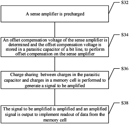
wherein during an offset compensation stage of the sense amplifier, the first PMOS transistor and the second PMOS transistor are configured to be in a diode connection mode, and the first NMOS transistor and the second NMOS transistor are configured to be in a cross-coupled amplification mode,
wherein during a pre-amplification stage of the sense amplifier, the first PMOS transistor and the second PMOS transistor are configured to be in a signal to be amplified receiving mode for receiving the signal to be amplified and the first NMOS transistor and the second NMOS transistor are configured in the cross-coupled amplification mode, the signal to be amplified being generated by charge sharing between charges in a parasitic capacitor of the first bit line or the second bit line and charges in a corresponding memory cell,
wherein during a write-back stage of the sense amplifier, the first PMOS transistor and the first NMOS transistor are configured as a first inverter, the second PMOS transistor and the second NMOS transistor are configured as a second inverter, and
the first inverter and the second inverter are configured to be in a latch mode, and
wherein the sense amplifier further comprises:
a first switch, a first end of the first switch being connected to the drain of the first PMOS transistor, and a second end of the first switch being connected to the gate of the first PMOS transistor;
a second switch, a first end of the second switch being connected to the drain of the second PMOS transistor, and a second end of the second switch being connected to the gate of the second PMOS transistor;
a third switch, a first end of the third switch being connected to the first end of the first switch, and a second end of the third switch being connected to the second end of the second switch; and
a fourth switch, a first end of the fourth switch being connected to the first end of the second switch, and a second end of the fourth switch being connected to the second end of the first switch.
|