| CPC G11C 7/062 (2013.01) [G11C 7/1069 (2013.01); G11C 7/1096 (2013.01); G11C 7/12 (2013.01); H03K 19/20 (2013.01)] | 20 Claims |
|
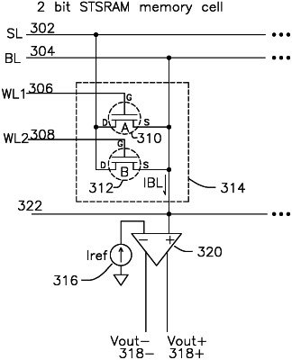
1. An arithmetic memory comprising:
a first Single Transistor Static Random Access Memory (STSRAM) having a source, drain, and gate, and storing a charge value which modifies a conductivity from the drain to the source when the gate is enabled;
a second STSRAM having a source, drain, and gate, and storing a charge value which modifies a conductivity from the drain to the source when the gate is enabled;
a select line (SL) coupled to the first STSRAM drain and also to the second STSRAM drain;
a current comparator amplifier (CCA) having a noninverting input and an inverting input, the CCA asserting a binary output when a sum of currents applied to the CCA noninverting input is greater than a current Iref applied to the inverting input of the CCA;
a Bit Line (BL) node coupled to the first STSRAM source, the second STSRAM source, and to the noninverting input of the CCA;
the CCA output configured to output at least one of an OR, NOR, AND, or NAND operation, and where the charge value of the first STSRAM and the charge value of the second STSRAM provides the sum of currents.
|