| CPC G11C 29/42 (2013.01) [G11C 16/102 (2013.01); G11C 16/26 (2013.01); G11C 29/12015 (2013.01); G11C 29/18 (2013.01); G11C 29/4401 (2013.01); G11C 2029/1202 (2013.01); G11C 2029/1204 (2013.01); G11C 2029/1802 (2013.01)] | 20 Claims |
|
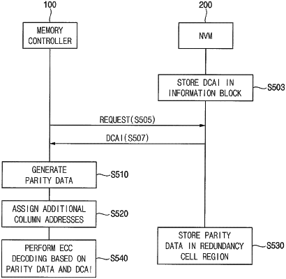
1. A nonvolatile memory device including:
a memory cell array including a normal cell region, a parity cell region and a redundancy cell region associated with repairing defective columns of the normal cell region and the parity cell region, the memory cell array including a plurality of nonvolatile memory cells coupled to first bit-lines and second bit-lines, the first bit-lines connected to the normal cell region and the parity cell region, the second bit-lines connected to the redundancy cell region;
a page buffer circuit connected to the memory cell array through the first bit-lines and the second bit-lines;
an address decoder connected to the memory cell array through a plurality of word-lines; and
a control circuit configured to control the page buffer circuit and the address decoder based on a command and an address received from a memory controller,
wherein the control circuit is configured to:
store a user data in the normal cell region,
perform a column repair on first defective bit-lines among the first bit-lines, each of the first defective bit-lines being associated with a given one of the defective columns, and
store at least a portion of a parity data in a region corresponding to the first defective bit-lines and the second bit-lines to which additional column addresses are assigned.
|