| CPC G11C 16/3495 (2013.01) [G11C 16/08 (2013.01); G11C 16/10 (2013.01); G11C 16/102 (2013.01); G11C 16/26 (2013.01); G11C 16/30 (2013.01); G11C 16/32 (2013.01); G11C 16/3454 (2013.01)] | 20 Claims |
|
1. A memory system, comprising:
nonvolatile memory devices respectively including a plurality of memory blocks, each of the plurality of memory blocks including a plurality of memory cells connected to a plurality of word lines; and
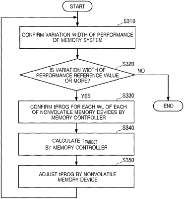
a memory controller confirming a programming time for each word line of each of the nonvolatile memory devices and calculating a target programming time on the basis of the programming time for each word line, wherein:
each of the nonvolatile memory devices receives the target programming time from the memory controller, and makes a respective adjustment of the programming time for each word line of the respective nonvolatile memory device on the basis of the target programming time, and
when the adjustment of the programming time for each respective nonvolatile memory device is completed, the memory controller confirms a variation width of a writing speed between the respective adjustments of the nonvolatile memory devices of the memory system for a predetermined time, and sets the target programming time as a final target programming time when the variation width of the writing speed is smaller than a reference value.
|