| CPC G11C 16/3495 (2013.01) [G11C 16/102 (2013.01); G11C 16/26 (2013.01); G11C 16/3404 (2013.01)] | 19 Claims |
|
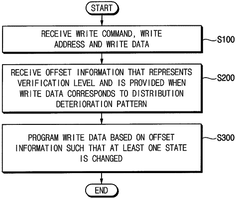
1. A method of writing data in a nonvolatile memory device, the method comprising:
receiving a write command, a write address and write data to be programmed;
receiving offset information representing a verification level, the receiving the offset information including,
checking an input/output (I/O) pattern of the write data and determining whether the write data corresponds to a distribution deterioration pattern based on results of the checking the I/O pattern of the write data,
in response to the write data not corresponding to the distribution deterioration pattern, not receiving the offset information, and
in response to the offset information not being received, programming the write data such that all of a plurality of states are maintained, the plurality of states corresponding to a distribution of threshold voltages of memory cells; and
in response to the offset information being received, programming the write data based on the offset information such that at least one state among the plurality of states included in the distribution of threshold voltages of memory cells in which the write data is stored is changed.
|