| CPC G11C 16/3459 (2013.01) [G11C 16/08 (2013.01); G11C 16/102 (2013.01); G11C 16/16 (2013.01); G11C 16/26 (2013.01); G11C 16/30 (2013.01); G11C 16/3495 (2013.01)] | 20 Claims |
|
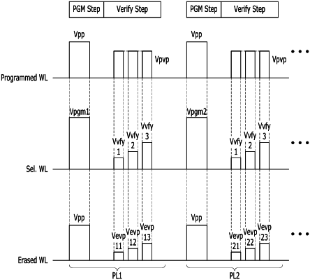
1. An operating method of a memory device, comprising:
a program operation of applying a program voltage to a selected word line to program selected memory cells connected to the selected word line;
a first verification operation of applying a first verification voltage to the selected word line and applying a first verification pass voltage to unselected word lines to verify a first program state of the selected memory cells; and
a second verification operation of applying a second verification voltage, which has a higher level than the first verification voltage, to the selected word line and applying a second verification pass voltage, which has a higher level than the first verification pass voltage, to the unselected word lines to verify a second program state higher than the first program state of the selected memory cells.
|