| CPC G11C 16/08 (2013.01) [G11C 11/5642 (2013.01); G11C 16/0483 (2013.01); G11C 16/24 (2013.01); G11C 16/26 (2013.01); G11C 16/30 (2013.01); G11C 16/32 (2013.01); G11C 16/3427 (2013.01)] | 20 Claims |
|
1. A semiconductor storage device, comprising:
a first memory cell electrically connected to a first bit line and a first word line;
a second memory cell electrically connected to a second bit line and the first word line; and
a first circuit configured to supply voltages to the first word line, wherein
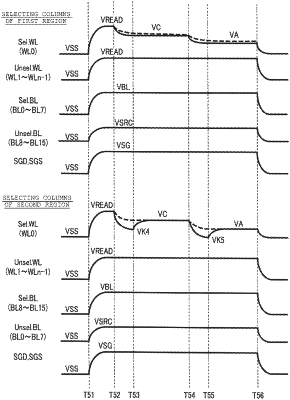
during a reading operation to read a page of memory cells including the first memory cell and the second memory cell, while the first memory cell is selected as a read target during a first time period, the first circuit supplies:
a first voltage to the first word line in an initial state during the first time period,
a second voltage that is greater than the first voltage to the first word line after supplying the first voltage,
a third voltage that is less than the second voltage to the first word line directly after supplying the second voltage; and
during the reading operation to read the page of memory cells including the first memory cell and the second memory cell, while the second memory cell is selected as the read target during a second time period that is different from the first time period, the first circuit supplies:
the first voltage to the first word line in an initial state during the second time period,
the second voltage to the first word line after supplying the first voltage,
a fourth voltage that is less than the third voltage and greater than the first voltage to the first word line directly after supplying the second voltage, and
the third voltage to the first word line directly after supplying the fourth voltage.
|