| CPC G11C 16/0433 (2013.01) [G11C 5/025 (2013.01); G11C 5/06 (2013.01); G11C 16/0483 (2013.01); G11C 16/08 (2013.01); G11C 16/10 (2013.01); G11C 16/102 (2013.01); G11C 16/26 (2013.01); G11C 16/30 (2013.01); G11C 16/32 (2013.01)] | 19 Claims |
|
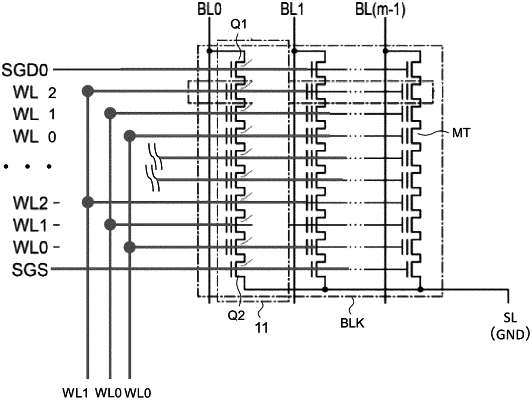
1. A memory system comprising:
a memory cell array having a plurality of strings, each of the plurality of strings having a plurality of memory cells connected in series;
a controller configured to perform control of transferring charges to be stored in the plurality of memory cells in a string of the plurality of strings or transferring charges according to stored data, between potential wells of a channel in the plurality of memory cells in the string; and
a plurality of first wiring lines connected to gates of the plurality of memory cells in the string, wherein
each of the plurality of first wiring lines is connected to gates of two or more of the plurality of memory cells in the string.
|