| CPC G11C 13/0026 (2013.01) [G11C 13/004 (2013.01); G11C 13/0028 (2013.01); G11C 13/0038 (2013.01); G11C 13/0069 (2013.01); H10N 70/826 (2023.02); H10N 70/841 (2023.02); G11C 2213/79 (2013.01)] | 40 Claims |
|
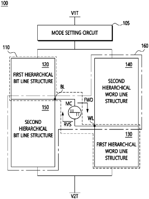
1. A variable resistive memory device comprising:
a memory cell including a first electrode, a second electrode and a memory layer, the memory layer interposed between the first electrode and the second electrode;
a first current-applying block configured to apply a first current to the first electrode that flows from the first electrode to the second electrode;
a second current-applying block configured to apply a second current to the second electrode that flows from the second electrode to the first electrode; and
a mode setting circuit configured to selectively provide any one of the first electrode of the first current-applying block and the second electrode of the second current-applying block with a first voltage,
wherein, when the memory cell is selected, the selected current-applying block, among the first current-applying block and the second current-applying block, is driven,
wherein a second voltage is applied to the second electrode when the first current-applying block is selected, and the second voltage is applied to the first electrode when the second current-applying block is selected, and
wherein the first voltage is higher than the second voltage by a threshold voltage.
|