| CPC G11C 11/4093 (2013.01) [G11C 5/147 (2013.01); G11C 7/02 (2013.01); G11C 7/1069 (2013.01); G11C 7/14 (2013.01); G11C 7/20 (2013.01); G11C 11/4072 (2013.01); G11C 11/4074 (2013.01); G11C 11/4076 (2013.01); G11C 11/4087 (2013.01); G11C 11/4091 (2013.01); G11C 11/4096 (2013.01); G11C 29/028 (2013.01); G11C 29/50 (2013.01); G11C 29/021 (2013.01); G11C 29/023 (2013.01); G11C 2207/2254 (2013.01)] | 20 Claims |
|
1. A memory system comprising:
a memory device; and
a memory controller configured to transmit input data to the memory device through a first data line and a second data line,
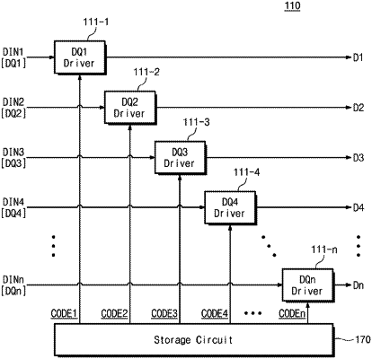
wherein the memory controller is further configured to store first to fourth codes in the memory device by performing a training operation, the first code including information of a first reference voltage level associated with the first data line, the second code including information of a first decision feedback equalization (DFE) level associated with the first data line, the third code including information of a second reference voltage level associated with the second data line, and the fourth code including information of a second DFE level associated with the second data line;
wherein the memory device comprises:
a first data line driver circuit configured to generate a first reference voltage set based on the first and second codes associated with the first data line, and to determine first bit values of the input data received through the first data line based on the first reference voltage set; and
a second data line driver circuit configured to generate a second reference voltage set based on the third and fourth codes associated with the second data line, and to determine second bit values of the input data received through the second data line based on the first reference voltage set.
|