US 11,862,231 B2
Memory device and operating method thereof
He-Zhou Wan, Shanghai (CN); Xiu-Li Yang, Shanghai (CN); Mu-Yang Ye, Nanjing (CN); and Yan-Bo Song, Shanghai (CN)
Assigned to TAIWAN SEMICONDUCTOR MANUFACTURING COMPANY, LTD, Hsinchu (TW); TSMC NANJING COMPANY LIMITED, Nanjing Province (CN); and TSMC CHINA COMPANY LIMITED, Shanghai (CN)
Filed by TAIWAN SEMICONDUCTOR MANUFACTURING COMPANY, LTD., Hsinchu (TW); TSMC Nanjing Company Limited, Nanjing (CN); and TSMC China Company Limited, Shanghai (CN)
Filed on Oct. 26, 2022, as Appl. No. 17/973,823.
Application 17/973,823 is a continuation of application No. 17/208,523, filed on Mar. 22, 2021, granted, now 11,514,974.
Claims priority of application No. 202110176842.2 (CN), filed on Feb. 9, 2021.
Prior Publication US 2023/0049698 A1, Feb. 16, 2023
This patent is subject to a terminal disclaimer.
Int. Cl. G11C 11/408 (2006.01); G11C 5/06 (2006.01); G11C 11/4074 (2006.01); G11C 11/4094 (2006.01)
CPC G11C 11/4085 (2013.01) [G11C 5/063 (2013.01); G11C 11/4074 (2013.01); G11C 11/4087 (2013.01); G11C 11/4094 (2013.01)] 20 Claims
OG exemplary drawing
 
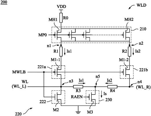
1. A memory device, comprising:
a first transistor coupled to a first word line at a first node;
a second transistor coupled to a second word line different from the first word line at a second node, wherein a control terminal of the first transistor is coupled to a control terminal of the second transistor; and
a third transistor coupled between a ground and a third node which is coupled to each of the first node and the second node,
wherein in a layout view, each of the first transistor and the second transistor has a first length along a direction, and
the first transistor, the third transistor and second transistor are arranged in order along the direction.