| CPC G11C 11/4074 (2013.01) [G11C 5/14 (2013.01); G11C 11/4096 (2013.01); G11C 11/4099 (2013.01)] | 18 Claims |
|
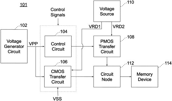
1. A driver circuit for operating a memory cell, adapted to be coupled to at least one memory cell through a respective output node, said driver circuit including:
a first circuit for supplying the memory cell with a first read reference voltage through the output node;
a second circuit for supplying the memory cell with a second read reference voltage through the output node; and
a third circuit for controlling an operation of the second circuit,
wherein a range of the second read reference voltage at the output node is wider than a range of the first read reference voltage at the output node during a read operation on the memory cell,
wherein the second circuit includes a plurality of PMOS transistors stacked in series between a connected voltage supply node and the output node, each of said PMOS transistors having a gate terminal coupled to a gate control node connected to the third circuit.
|