| CPC G11C 11/4074 (2013.01) [G11C 7/1063 (2013.01); G11C 7/1069 (2013.01); G11C 11/4096 (2013.01)] | 20 Claims |
|
1. A memory device, comprising:
a memory array comprising a plurality of memory cells;
a control circuit operatively coupled to the memory array, the control circuit configured to:
receive a read request for data;
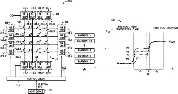
apply a plurality of read voltages to the memory array based on the read request, wherein the plurality of read voltages are applied in parallel via a plurality of partitions included in the memory array, and wherein each voltage value of the plurality of read voltages is different from each other;
perform a data analysis for a first set of data read based on the application of the plurality of read voltages;
derive a demarcation bias voltage (VDM) based on the data analysis; and
apply the VDM to the memory array to read a second set of data.
|