| CPC G11C 11/1673 (2013.01) [G06F 17/142 (2013.01); G11C 11/1653 (2013.01); G11C 11/1675 (2013.01); G11C 11/1697 (2013.01)] | 25 Claims |
|
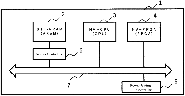
1. A device, comprising:
an MRAM configured to include multiple memory cells separated into multiple regions including selection transistors and MTJs;
a nonvolatile CPU configured to include a nonvolatile memory;
a nonvolatile FPGA-ACC configured to include a nonvolatile memory and execute a part of operations on the nonvolatile CPU in parallel; and
a power-gating controller configured to control power supply to each memory cell in the MRAM, the nonvolatile CPU, and the nonvolatile FPGA-ACC,
wherein the device is a single-chip microcomputer having the MRAM, the nonvolatile CPU, the nonvolatile FPGA-ACC, and the power-gating controller.
|