| CPC G11C 13/003 (2013.01) [G11C 13/004 (2013.01); G11C 13/0026 (2013.01); G11C 13/0038 (2013.01); G11C 13/0069 (2013.01)] | 37 Claims |
|
1. An apparatus comprising:
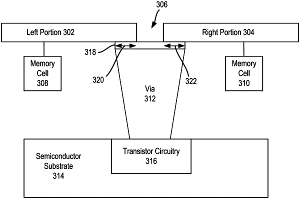
an access line having a first portion, a second portion, and a central portion, wherein:
the first and second portions are on opposite sides of the central portion, and each of the first and second portions is configured to access at least one memory cell of a memory array; and
the access line includes a first resistive layer in the first portion and a second resistive layer in the second portion, each of the first and second resistive layers is configured as part of the access line;
at least one via electrically connected, by the central portion of the access line, to the first and second portions of the access line; and
a driver electrically connected to the at least one via, wherein the driver is configured to generate a voltage on the first portion to access a first memory cell, the first memory cell located in a portion of the memory array underlying or overlying the first resistive layer, and to generate a voltage on the second portion to access a second memory cell, the second memory cell located in a portion of the memory array underlying or overlying the second resistive layer.
|