| CPC G11B 5/3909 (2013.01) [G01R 33/093 (2013.01); G11B 5/3166 (2013.01); G11B 5/332 (2013.01); G11B 5/3912 (2013.01); G11B 5/3948 (2013.01); Y10T 29/49036 (2015.01)] | 9 Claims |
|
1. A method comprising:
selecting first design parameter values for a spin injector and for a first interface resistance between the spin injector and a channel layer;
selecting second design parameter values for a detector and for a second interface resistance between the detector and the channel layer;
selecting third design parameter values for the channel layer such that the third design parameter values comport with the first design parameter values and the second design parameter values, the selection of the third design parameter values comprising:
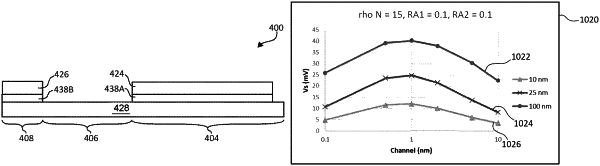
measuring different detector-channel voltage values for different thickness values for the channel layer between a predetermined low thickness value and a predetermined high thickness value; and
selecting a thickness value of the different thickness values that provides a highest detector-channel voltage value of the measured different detector-channel voltage values.
|