| CPC G09G 3/3291 (2013.01) [G09G 3/2096 (2013.01); G09G 2310/0291 (2013.01); G09G 2320/0276 (2013.01); G09G 2320/041 (2013.01); G09G 2320/0626 (2013.01); G09G 2320/0673 (2013.01); G09G 2330/028 (2013.01); G09G 2354/00 (2013.01); G09G 2360/16 (2013.01)] | 20 Claims |
|
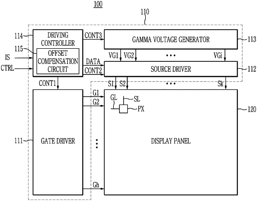
1. A semiconductor device comprising:
an offset compensation circuit configured to:
obtain first data comprising first low-order bit data, second low-order bit data and high-order bit data, select two compensation values from among a plurality of compensation values based on the first low-order bit data,
identify a final compensation value by interpolating the two compensation values based on the second low-order bit data, and
compensate the final compensation value to generate second data; and
a source driver configured to interpolate and output two gamma voltages from among a plurality of gamma voltages based on the second data.
|