| CPC G09G 3/3266 (2013.01) [G09G 3/3233 (2013.01); G09G 2300/0842 (2013.01); G09G 2310/0286 (2013.01); G09G 2310/08 (2013.01); G09G 2320/0233 (2013.01); G09G 2320/041 (2013.01); G09G 2320/045 (2013.01)] | 20 Claims |
|
1. A scan driver comprising a plurality of stages,
wherein each of the plurality of stages comprises:
a node controller configured to control a voltage level of a first control node;
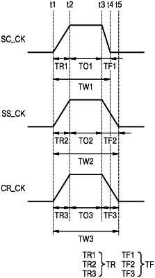
a first output controller comprising a first pull-up transistor connected between a first clock input terminal configured to receive a first clock signal, and a first output terminal and configured to output the first clock signal as a first scan signal in response to the first control node having an on-voltage level;
a second output controller comprising a second pull-up transistor connected between a second clock input terminal and configured to receive a second clock signal, and a second output terminal and configured to output the second clock signal as a second scan signal in response to the first control node having the on-voltage level; and
a third output controller comprising a third pull-up transistor connected between a third clock input terminal configured to receive a third clock signal, and a third output terminal and configured to output the third clock signal as a carry signal in response to the first control node having the on-voltage level,
wherein a falling time of the first clock signal is shorter than falling times of the second clock signal and the third clock signal.
|