| CPC G09G 3/3266 (2013.01) [G09G 3/3275 (2013.01); G09G 2300/0842 (2013.01); G09G 2310/0278 (2013.01); G09G 2330/021 (2013.01)] | 19 Claims |
|
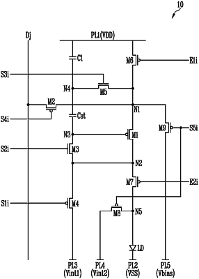
1. A display device comprising:
a pixel connected to first to fifth scan lines, first and second emission control lines, and a data line;
a scan driver which supplies first to fifth scan signals to the first to fifth scan lines, respectively;
an emission driver which supplies first and second emission control signals to the first and second emission control lines, respectively; and
a data driver which supplies a data signal to the data line,
wherein the pixel comprises:
a light emitting element;
a first transistor connected between a first node and a second node and which generates a driving current flowing from a first power supply line, through which a first power supply voltage is supplied, to a second power supply line, through which a second power supply voltage is supplied, and flowing through the light emitting element;
a second transistor connected between the data line and the first node and which is turned on in response to the fourth scan signal;
a third transistor connected between the second node and a third node and which is turned on in response to the second scan signal, the third node being connected to a gate electrode of the first transistor;
a fourth transistor connected between the second node and a third power line through which a third power supply voltage is supplied, and which is turned on in response to the first scan signal;
a fifth transistor connected between the first node and a fourth node and which is turned on in response to the third scan signal;
a sixth transistor connected between the first power line and the first node and which is turned off in response to the first emission control signal supplied to the first emission control line;
a storage capacitor connected between the third node and the fourth node; and
a first capacitor connected between the first power line and the fourth node,
wherein the third transistor and the fifth transistor are oxide semiconductor transistors.
|