| CPC G09G 3/3266 (2013.01) [G09G 3/3677 (2013.01); G11C 19/28 (2013.01); G09G 2300/0852 (2013.01); G09G 2310/0286 (2013.01)] | 16 Claims |

|
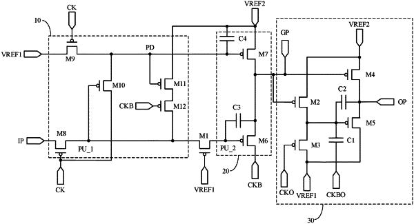
1. A driving method of a shift register, comprising: at a first refresh frequency, one display frame comprising a data refresh stage and a data retention stage, wherein the data retention stage comprises a denoising retention stage and a denoising enhancement stage alternately arranged;
at the data refresh stage, loading an input signal with a pulse level to an input signal end, loading a control clock pulse signal to a control clock signal end, loading a noise reduction clock pulse signal to a noise reduction clock signal end, loading a fixed voltage signal to a first reference signal end, loading a fixed voltage signal to a second reference signal end, and controlling a cascade signal end of the shift register to output a cascade signal with a pulse level, and control a driving signal end of the shift register to output a driving signal with a pulse level;
at the denoising retention stage, loading a fixed voltage signal to the input signal end, loading a fixed voltage signal to the control clock signal end, loading a fixed voltage signal to the noise reduction clock signal end, loading a fixed voltage signal to the first reference signal end, loading a fixed voltage signal to the second reference signal end, and controlling the cascade signal end to output a fixed voltage signal, and controling the driving signal end to output a fixed voltage signal; and
at the denoising enhancement stage, loading a fixed voltage signal to the input signal end, loading a fixed voltage signal to the control clock signal end, loading a clock pulse signal to the noise reduction clock signal end, loading a fixed voltage signal to the first reference signal end, loading a fixed voltage signal to the second reference signal end, and controlling the cascade signal end to output a fixed voltage signal, and controlling the driving signal end to output a fixed voltage signal.
|