| CPC G09G 3/32 (2013.01) [G09G 2300/043 (2013.01); G09G 2300/0426 (2013.01); G09G 2300/0819 (2013.01); G09G 2300/0842 (2013.01); G09G 2300/0861 (2013.01); G09G 2310/08 (2013.01); G09G 2320/0233 (2013.01)] | 26 Claims |
|
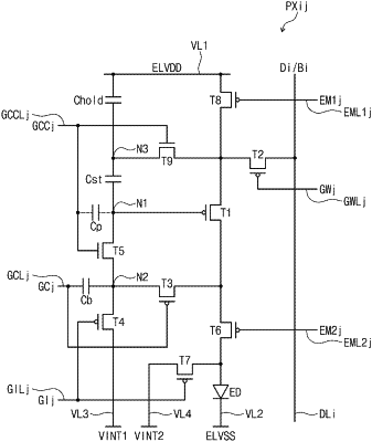
1. A pixel comprising:
a light emitting element;
a first transistor including a first electrode electrically connected to a first voltage line which supplies a first driving voltage, a second electrode electrically connected to the light emitting element, and a gate electrode connected to a first node;
a second transistor connected between the first node and a second node and including a gate electrode connected to a first scan line;
a third transistor connected between the second electrode of the first transistor and the second node and including a gate electrode connected to a second scan line; and
a boosting capacitor connected between the second node and the second scan line.
|