| CPC G09G 3/2092 (2013.01) [G02F 1/1333 (2013.01); G02F 1/13454 (2013.01); G02F 1/1345 (2013.01); G02F 2201/56 (2013.01); G09G 3/3611 (2013.01); G09G 2300/0426 (2013.01); G09G 2310/0202 (2013.01); G09G 2310/0281 (2013.01)] | 20 Claims |
|
1. A display device, comprising:
a lower receiving container;
an upper receiving container formed on the lower receiving container; and
a display panel formed between the lower receiving container and the upper receiving container, the display panel comprising a display substrate in which at least a portion of an edge of the display substrate has an arc shape,
wherein the display substrate comprises:
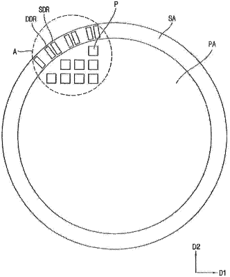
a plurality of pixels arranged in a pixel area in which at least a portion of an edge of the pixel area has an arc shape;
a driving circuit formed in a peripheral area surrounding the pixel area and overlapped by the upper receiving container, the driving circuit comprising a plurality of scan circuits and a plurality of data circuits alternately arranged along a boundary between the pixel area and the peripheral area;
a plurality of scan lines formed in the pixel area, the scan lines extending in a first direction; and
a plurality of scan connecting lines each configured to electrically connect each of the scan circuits to each of the scan lines,
wherein a first portion of each of the scan connecting lines is overlapped by the upper receiving container, and
wherein a second portion of each of the scan connecting lines, which does not overlap the upper receiving container, extends in a direction different from the first direction and is connected to each of the scan lines,
wherein a distance between a lower portion of a scan circuit of the plurality of scan circuits and a lower portion of a data circuit of the plurality of data circuits is less than a distance between an upper portion of the scan circuit and an upper portion of the data circuit.
|