| CPC G06F 30/398 (2020.01) [G06F 30/392 (2020.01)] | 20 Claims |
|
1. A computer-implemented method comprising:
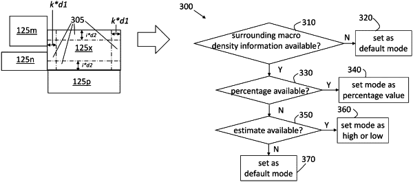
defining a plurality of border regions of a layer of a macro of an integrated circuit, wherein a first border region comprises a depth defined by a multiple of a width of a tile used to select an area of the integrated circuit for implementation of a design rule check and a second border region overlapping the first border region comprises a depth defined by a multiple of a length of the tile;
separately setting, for each border region of the plurality of border regions, a fill mode, the fill mode indicating a fill percentage value or level of fill to be implemented in the respective border region of the layer of the macro; and
performing a fill of the border regions of the layer of the macro based on the respective fill modes, wherein the integrated circuit is finalized and fabricated based on the performing of the fill and passing the design rule check.
|